Purpose
The RT5784A is a current mode step-down converter with the input voltage range from 2.5V to 6V and provides 2A output current. This document explains the function and use of the RT5784A evaluation board (EVB), and provides information to enable operation, modification of the evaluation board and circuit to suit individual requirements.
Introduction
General Product Information
The RT5784A is a high-performance, Advanced Constant On-Time (ACOT™) monolithic synchronous step-down DC/DC converter that can deliver up to 2A output current from a 2.5V to 6V input supply. The proprietary ACOT control architecture features quick transient response and provides stable operation with small ceramic output capacitors and without complicated external compensation. The switching ripple voltage is easily smoothed-out by small package filtering elements due to a constant switching frequency of 1.5MHz and the maximum duty cycle of 100% allows the device to operate at low dropout use. With internal low on-resistance power switches and extremely low quiescent current, the RT5784A displays excellent efficiency and good behavior across a range of applications. Cycle-by-cycle current limit provides protection against shorted outputs, input under-voltage lock-out, output under-voltage protection, and thermal shutdown provide safe and smooth operation in all operating conditions. The RT5784A is available in the WDFN-8JL 2x1.5 (FC) package.
Product Feature
- Dramatically Fast Transient Response
- Steady 1.5MHz ±200kHz Switching Frequency
- Very Low Input Quiescent and Shutdown Currents
- Advanced COT Control Loop Design
- Optimized for Ceramic Output Capacitors
- 2.5V to 6V Input Voltage Range
- Accurate Voltage Reference 0.6V ±2%
- Integrated 100mΩ/60mΩ MOSFETs
- Internal Start-Up into Pre-biased Outputs
- Power Good Indicator
- Enable Control
- Over-Current and Over-Temperature Protections
- Under-Voltage Protection with Hiccup Mode
- RoHS Compliant and Halogen Free
Key Performance Summary Table
|
Key Features
|
Evaluation Board Number: PCB078_V1
|
|
Default Input Voltage
|
5V
|
|
Max Output Current
|
2A
|
|
Default Output Voltage
|
1.0V
|
|
Default Marking & Package Type
|
RT5784AGQWF, WDFN-8JL 2x1.5 (FC)
|
|
Operation Frequency
|
Steady 1.5MHz at all loads
|
Bench Test Setup Conditions
Headers Description and Placement
Carefully inspect all the components used in the EVB according to the following Bill of Materials table, and then make sure all the components are undamaged and correctly installed. If there is any missing or damaged component, which may occur during transportation, please contact our distributors or e-mail us at evb_service@richtek.com.
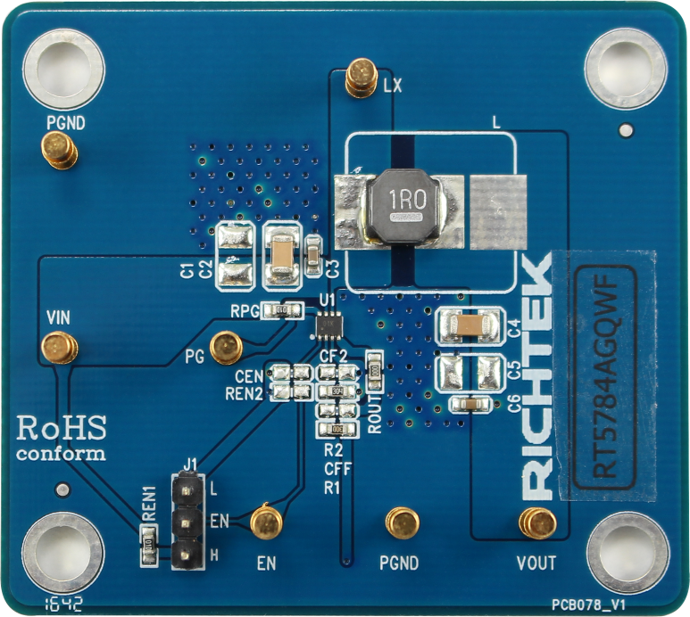
Test Points
The EVB is provided with the test points and pin names listed in the table below.
|
Test point/
Pin name
|
Signal
|
Comment (expected waveforms or voltage levels on test points)
|
|
VIN
|
Input voltage
|
Supply Input. Supplies the power to the internal control circuit as well as the power switches of the device. Drive VIN with a 2.5V to 6V power source and bypass VIN to PGND with a suitably large capacitor to eliminate noise on the input to the IC.
|
|
EN
|
Enable test point
|
Enable Control Input. Connecting this pin to logic high can enable the device and connecting this pin to GND can disable the device.
|
|
PGND
|
Ground
|
Power Ground. This pin must be soldered to a large PCB and connected to analog ground for maximum power dissipation.
|
|
FB
|
Feedback voltage input
|
Feedback Voltage Input. This pin is used to set the desired output voltage via an external resistive divider. The feedback reference voltage is 0.6V typically.
|
|
PGOOD
|
Power Good test point
|
Power Good Indicator Output. This pin is an open-drain logic output that is pulled to ground when the output voltage is lower or higher than its specified threshold under the conditions of UVP, OTP, dropout, EN shutdown, or during slow start.
|
|
VOUT
|
Output Voltage
|
Output Voltage Sense Input. This pin is used to monitor and adjust output voltage for superior load transient regulation.
|
|
LX
|
Switch node test point
|
Switch Node. LX is the switching node that supplies power to the output and connect the output LC filter from LX to the output load.
|
|
AGND
|
Ground
|
Analog Ground. Provides the ground return path for control circuitry and internal reference.
|
Power-up & Measurement Procedure
1. Connect input power (2.5V < VIN < 6V) and input ground to VIN and GND test pins respectively.
2. Connect positive end and negative terminals of load to VOUT and GND test pins respectively.
3. There is a 3-pin header “EN” for enable control. To use a jumper at “H” option to tie EN test pin to input power VIN for enabling the device. Inversely, to use a jumper at “L” option to tie EN test pin and ground GND for disabling the device.
4. Verify the output voltage (approximately 1.0V) between VOUT and GND.
5. Connect an external load up to 2A to the VOUT and GND terminals and verify the output voltage and current.
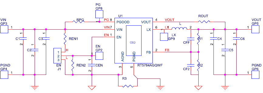
Output Voltage Setting
Set the output voltage with the resistive divider (R1, R2) between VOUT and GND with the midpoint connected to FB. The output is set by the following formula:
VOUT = VFB x (1 + R1 / R2)
Schematic, Bill of Materials & Board Layout
EVB Schematic Diagram
Bill of Materials
|
Reference
|
Qty
|
Part number
|
Description
|
Package
|
Manufacturer
|
|
U1
|
1
|
RT5784AGQWF
|
RT5784AGQWF
|
WDFN-8JL 2x1.5 (FC)
|
RICHTEK
|
|
REN2, CF2, CEN, CFF, C1, C5
|
6
|
NC
|
NC
|
|
|
|
C2, C4
|
2
|
10µF/1210,16V
|
10µF/25V/X5R/1206
|
|
TDK
|
|
C3, C6
|
2
|
0.1µF/0603
|
0.1μF/±10%/50V/X7R/0603
|
|
TDK
|
|
J1
|
1
|
EN
|
單排排針
|
|
|
|
L
|
1
|
1µH
|
1.0uH/4.2A/6mm*6mm
|
6x6x4.5mm
|
TAIYO YUDEN
|
|
REN1, RPG
|
2
|
100k/0603
|
100k/0603
|
|
WALSIN
|
|
ROUT
|
1
|
0R
|
0R
|
|
WALSIN
|
|
R1
|
1
|
200k/0603
|
200k/0603
|
|
WALSIN
|
|
R2
|
1
|
300k/0603
|
300k/0603
|
|
WALSIN
|
|
R3
|
1
|
0 ohm
|
0R
|
|
WALSIN
|
PCB Layout
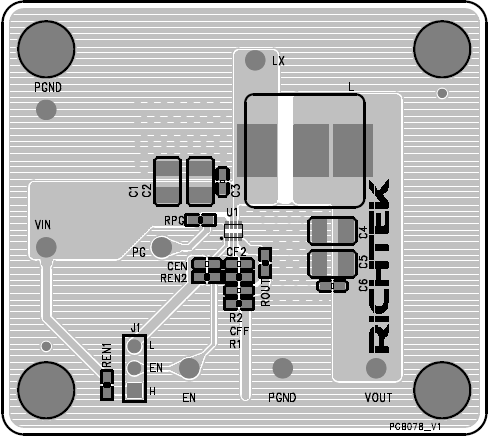
Top View (1st layer)

PCB Layout—Inner Side (2nd Layer)

PCB Layout—Inner Side (3rd Layer)
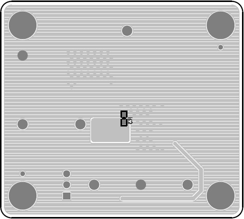
Bottom View (4th Layer)